
News
Home > News > Technical Documentation
Technical Documentation


Effects of EOS (Electrical Overstress) on components
2020/10/30

EOS causes two basic types of failures
– Fatal failure due to overstress
● high levels of induced signals
– Latch-Up
● induced voltages outside of supply rails
● causes overheating leading to failure
● sometimes recoverable after power cycling
EOS damage of IC (Image 1)
● EOS signals deliver significant amounts of energy to the devices
● Damage to the devices is often manifested as massive meltdown
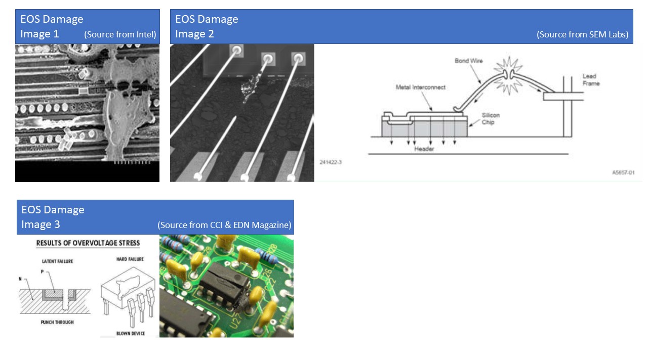
EOS and Wire Bond (Image 2)
● Massive energy delivered by EOS can melt wires inside the packaged device
● Most problematic is latent failure when the wire is weakened but the damage is not detected during the device test
● Such weakened device can fail in product' s use
EOS and Latent Damage (Image 3)
● EOS can be more prone to cause latent damage than ESD
● Large energy delivered by EOS weakens the structure, the features and the geometry
● Weakened elements may still perform adequately during final test but fail in use when even the slightest normally acceptable stress is applied
Therefore, EOS phenomenon will shorten or even damage the life cycle of products. From the engineering development and test development stage to the mass production stage, to confirm there are no any EOS phenomenon happen will definitely improve the quality of products and reduce the loss of testing costs.
– Fatal failure due to overstress
● high levels of induced signals
– Latch-Up
● induced voltages outside of supply rails
● causes overheating leading to failure
● sometimes recoverable after power cycling
EOS damage of IC (Image 1)
● EOS signals deliver significant amounts of energy to the devices
● Damage to the devices is often manifested as massive meltdown
EOS and Wire Bond (Image 2)
● Massive energy delivered by EOS can melt wires inside the packaged device
● Most problematic is latent failure when the wire is weakened but the damage is not detected during the device test
● Such weakened device can fail in product' s use
EOS and Latent Damage (Image 3)
● EOS can be more prone to cause latent damage than ESD
● Large energy delivered by EOS weakens the structure, the features and the geometry
● Weakened elements may still perform adequately during final test but fail in use when even the slightest normally acceptable stress is applied
Therefore, EOS phenomenon will shorten or even damage the life cycle of products. From the engineering development and test development stage to the mass production stage, to confirm there are no any EOS phenomenon happen will definitely improve the quality of products and reduce the loss of testing costs.
